


Texas Instruments TMS320F280x, TMS320C280x, & TMS320F2801x DSPs
Texas Instruments TMS320F280x, TMS320C280x, and TMS320F2801x Digital Signal Processors are part of the DSP generation of highly integrated, high-performance solutions for demanding control applications. The TI TMS320F280x, TMS320C280x, and TMS320F2801x DSPs feature a low-power 1.8V core, 3.3V I/O, and high-performance static CMOS technology.
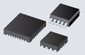
The TMS320F280x, TMS320C280x, and TMS320F2801x Digital Signal Processors use a boundary scan architecture with up to 16 PWM outputs and low-power modes. The TMS320F280x, TMS320C280x, and TMS320F2801x are available in thin quad flatpack (PZ) and MicroStar BGA™ packages.
Features
- High-performance static CMOS technology
- 100MHz (10ns cycle time)
- 60MHz (16.67ns cycle time)
- Low-power (1.8V core, 3.3V I/O) design
- JTAG boundary scan support
- IEEE Standard 1149.1-1990 standard test access port and boundary scan architecture
- High-performance 32-bit CPU (TMS320C28x)
- 16 x 16 and 32 x 32 MAC operations
- 16 x 16 dual MAC
- Harvard bus architecture
- Atomic operations
- Fast interrupt response and processing
- Unified memory programming model
- Code-efficient (in C/C++ and Assembly)
- On-chip memory
- F2809: 128K x 16 flash, 18K x 16 SARAM
- F2808: 64K x 16 flash, 18K x 16 SARAM
- F2806: 32K x 16 flash, 10K x 16 SARAM
- F2802: 32K x 16 flash, 6K x 16 SARAM
- F2801: 16K x 16 flash, 6K x 16 SARAM
- F2801x: 16K x 16 flash, 6K x 16 SARAM
- 1K x 16 OTP ROM (flash devices only)
- C2802: 32K x 16 ROM, 6K x 16 SARAM
- C2801: 16K x 16 ROM, 6K x 16 SARAM
- Boot ROM (4K x 16)
- With software boot modes (via SCI, SPI, CAN, I2C, and parallel I/O)
- Standard math tables
- Clock and system control
- On-chip oscillator
- Watchdog timer module
- Any GPIO A pin can be connected to one of the three external core interrupts
- Peripheral Interrupt Expansion (PIE) block that supports all 43 peripheral interrupts
- Endianness: Little endian
- 128-bit security key/lock
- Protects flash/OTP/L0/L1 blocks
- Prevents firmware reverse-engineering
- Three 32-bit CPU timers
- Enhanced control peripherals
- Up to 16 PWM outputs
- Up to 6 HRPWM outputs with 150ps MEP resolution
- Up to four capture inputs
- Up to two quadrature encoder interfaces
- Up to six 32-bit/six 16-bit timers
- Serial port peripherals
- Up to 4 SPI modules
- Up to 2 SCI (UART) modules
- Up to 2 CAN modules
- One Inter-Integrated-Circuit (I2C) bus
- 12-bit ADC, 16 channels
- 2 x 8 channel input multiplexer
- Two sample-and-hold
- Single/simultaneous conversions
- Fast conversion rate:
- 80ns - 12.5MSPS (F2809 only)
- 160ns - 6.25MSPS (280x)
- 267ns - 3.75MSPS (F2801x)
- Internal or external reference
- Up to 35 individually programmable, multiplexed GPIO pins with input filtering
- Advanced emulation features
- Analysis and breakpoint functions
- Real-time debugging via hardware
- Development support includes
- ANSI C/C++ compiler/assembler/linker
- Code Composer Studio™ IDE
- SYS/BIOS
- Digital motor control and digital power software libraries
- Low-power modes and power savings
- IDLE, STANDBY, and HALT modes supported
- Disable individual peripheral clocks
- Package options
- Thin quad flatpack (PZ)
- MicroStar BGA™ (GGM, ZGM)
- Temperature options
- A: -40°C to +85°C (PZ, GGM, ZGM)
- S: -40°C to +125°C (PZ, GGM, ZGM)
- Q: -40°C to +125°C (PZ)
- (AEC-Q100 qualification for automotive applications)
Applications
- Motor drive and control
- Digital power
Functional Block Diagram

Related Products
Texas Instruments TMS320F2805x Piccolo™ Microcontrollers
Provides the power of the C28x™ core & CLA coupled w/highly integrated control peripherals.

Texas Instruments TMS320F2807x 32-Bit Microcontrollers (MCUs)
These MCUs are well suited for advanced closed-loop control applications.
Paskelbta: 2020-11-09
| Atnaujinta: 2025-04-08