


Texas Instruments CD74HCx4511 BCD-to-7 Segment Latch/Decoder/Drivers
Texas Instruments CD74HCx4511 BCD-to-7 Segment Latch/Decoder/Drivers have four address inputs (D0−D3), an active low blanking (/BL) input, a lamp-test (/LT) input, and a latch-enable (/LE) input. When these inputs are high, it enables the latches to store the BCD inputs. When /LE is low, the latches are disabled, making the outputs transparent to the BCD inputs.
The Texas Instruments CD74HCx4511 devices have standard-size output transistors but can source (at standard VOH levels) 7.5mA at 4.5V and up to 10mA at 6V.
Features
- VCC operation
- CD74HC4511: 2V to 6V
- CD74HCT4511: 4.5V to 5.5V
- High-output sourcing capability
- CD74HCT4511: 7.5mA at 4.5V
- CD74HC4511: 10mA at 6V
- Input latches for BCD code storage
- Lamp test and blanking capability
- Balanced propagation delays and transition times
- Significant power reduction compared to LSTTL logic ICs
- CD74HC4511 has a high noise immunity, NIL or NIH = 30% of VCC at VCC = 5V
- CD74HCT4511
- Direct LSTTL input logic compatibility, VIL = 0.8V maximum, VIH = 2V minimum
- CMOS input compatibility, II ≤ 1μA at VOL, VOH
Applications
- Data routing
- Memory address decoding
Additional Resources
- Application Note: Designing With Logic
- Application Note: Implications of Slow or Floating CMOS Inputs
- Application Note: Understanding and Interpreting Standard-Logic Data Sheets
- Application Note: Using High-Speed CMOS and Advanced CMOS in Systems With Multiple VCC
- Selection Guide: Logic Guide
- User Guide: LOGIC Pocket Data Book
Functional Block Diagram

Development Tool
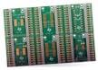
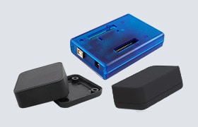
Texas Instruments 14-24-LOGIC-EVM Logic Evaluation Module (EVM)
Generic evaluation module developed to support any TI logic leaded device in a 14 to 24 pin count.
Paskelbta: 2025-04-30
| Atnaujinta: 2025-05-08