


Microchip Technology MCP47CXBXX Digital-to-Analog Converters
Microchip Technology MCP47CxBx Digital-to-Analog Converters are Single and Dual-Channel 8-bit, 10-bit, and 12-bit buffered voltage output DAC ICs, with volatile or MTP (Multi Time Programmable) memory and an I2C serial interface. The user can write the integrated MTP memory up to 32 times for each specific register. The Microchip Technology converters require a high-voltage level on the HVC pin, typically 7.5V, to successfully program the desired memory location. The nonvolatile memory includes power-up output values, device configuration registers, and general-purpose memory.
The VREF pin, the device VDD, or the internal bandgap voltage can be selected as the DAC’s reference voltage. When VDD is selected, VDD is internally connected to the DAC reference circuit.
When the VREF pin is used with an external voltage reference, the user can select between a gain of 1 or 2 and have the reference buffer enabled or disabled. When the gain is 2, the VREF pin voltage should be limited to a maximum of VDD/2.
These devices have a two-wire I2C-compatible serial interface for Standard (100kHz), Fast (400kHz), or High-Speed (1.7MHz and 3.4MHz) modes.
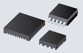
The MCP47CxBx DAC ICs are offered in three compact package options (MSOP-10, DFN-10, and QFN-16) for design flexibility.
Features
- Memory options
- Volatile memory - MCP47CVBXX
- Nonvolatile memory - MCP47CMBXX
- Non-volatile memory (MTP) size - 32 locations
- 1 LSb Integral Non-linearity (INL) specification
- -40°C to 125°C extended temperature range
- Operating voltage range
- 2.7V to 5.5V - full specifications
- 1.8V to 2.7V - reduced device specifications
- Output voltage resolutions
- 8-bit - MCP47CXB0X (256 steps)
- 10-bit - MCP47CXB1X (1024 steps)
- 12- bit - MCP47CXB2X (4096 steps)
- DAC voltage reference source options
- Device VDD
- External VREF pin (buffered or unbuffered)
- Internal band gap of 1.227V typical
- Output gain options
- 1x unity
- 2x available when not using internal VDD as a voltage source
- Power-on/Brown-out reset (POR/BOR) protection
- Power-down modes
- Disconnects output buffer (high-impedance)
- Selection of VOUT pull-down resistors (100kΩ or 1kΩ)
- I2C interface
- Slave address options: register-defined address with two physical address select pins (package dependent)
- Standard (100kbps), fast (400kbps), and high-speed (up to 3.4Mbps) modes
- Package types
- Dual 16-lead 3 x 3 QFN, 10-lead MSOP, and 10-lead 3 x 3 DFN
- Single 16-lead 3 x 3 QFN, 10-lead MSOP, and 10-lead 3 x 3 DFN
Applications
- Set-point or offset trimming
- Sensor calibration
- Low-power portable instrumentation
- PC peripherals
- Data acquisition systems
Paskelbta: 2018-10-08
| Atnaujinta: 2022-12-12